EMS Manufacturer for Automotive & New Energy

English

English
EMS Manufacturer for Automotive & New Energy
English
English
When a product team must build five circuit designs in batches of 50 to 2,000 units, standard mass production is often too rigid and too expensive. PCBA Contract Manufacturing high mix low volume services are designed for this gap. They support frequent design changes, different bill-of-materials files, short production runs, and strict testing requirements. A suitable partner can combine high-mix low-volume PCB assembly, controlled sourcing, fast engineering review, and complete traceability in one process. For medical devices, industrial controls, communication equipment, and smart hardware, this model reduces launch risk while keeping production flexible.
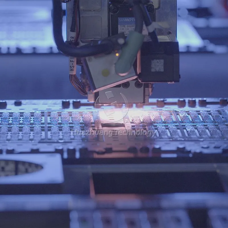
High-mix, low-volume PCBA manufacturing means producing many different printed circuit board assembly designs in relatively small quantities.
“High mix” refers to the number of product types, board revisions, component combinations, or assembly programs. “Low volume” refers to the quantity of each design. For example, a contract manufacturer may produce:
This is different from high-volume manufacturing, where one board may run for hundreds of thousands of units with few changes.
A high-mix production line must manage more than placement speed. It must control:
For this reason, low-volume electronics manufacturing depends heavily on process control and engineering discipline. A fast line without accurate change management can create more defects than it prevents.
The need for flexible electronics production is growing because product development cycles are shorter. Startups, research teams, and established manufacturers may release several product versions before market demand becomes clear.
A typical product may pass through these stages:
Each stage may use a different PCB layout, component list, firmware version, or test fixture. A production partner must maintain control across all stages instead of treating every order as a separate project.
For example, a power control board may include:
A small mistake in component substitution or firmware loading can cause field failures. Proper PCBA Contract Manufacturing therefore combines procurement, assembly, inspection, testing, and documentation.
The complete process begins before the first component is placed. Each stage should produce a clear record for the next stage.
The manufacturer reviews the following files:
The engineering team checks whether the BOM contains complete manufacturer part numbers, approved alternatives, package information, and lifecycle status.
A useful RFQ review should identify:
A design review can be completed using DFM and DFA rules. Common review items include solder pad geometry, component spacing, fiducial placement, thermal relief, panelization, and assembly orientation.
In high-mix production, procurement risk often has a greater effect than machine speed. A single unavailable microcontroller can stop an entire assembly program.
A controlled sourcing plan should classify components by risk:
For each high-risk component, the manufacturer should confirm:
Counterfeit screening may include marking inspection, package measurement, X-ray examination, decapsulation, or electrical comparison. Not every component requires destructive testing, but high-value or high-risk parts may justify additional controls.
The bare PCB should be checked against the customer’s drawings and agreed specifications.
Typical inspection items include:
For controlled-impedance boards, the fabrication supplier may provide impedance test coupons. The actual target depends on the design, but common single-ended and differential impedance requirements include 50 Ω and 90–100 Ω ranges.
Inspection equipment may include:
The board surface finish may be HASL, lead-free HASL, ENIG, immersion tin, or OSP. ENIG is often selected for fine-pitch components because it provides a relatively flat surface for small pads and QFN or BGA assembly.
Surface-mount technology is used for most modern PCB assemblies. Through-hole technology remains important for high-current terminals, transformers, switches, connectors, and mechanically stressed parts.
A controlled SMT process may include:
Solder paste should be stored according to the supplier’s requirements. A common control range is 2 °C to 10 °C for refrigerated storage, although the exact requirement depends on the paste specification.
The reflow profile must match the solder paste and component requirements. A lead-free SAC alloy profile may use:
These numbers are process examples, not universal settings. The final profile must be verified with thermocouples placed on representative heavy and light components.
For moisture-sensitive devices, floor life must be controlled according to the component’s MSL classification. When required, baking may be performed before assembly. This reduces the risk of package cracking, also known as “popcorn” damage, during reflow.
Inspection should not depend on one machine. Different inspection methods find different problems.
SPI checks solder paste volume, height, area, offset, and bridging before component placement. It can detect insufficient paste before the board reaches the reflow oven.
AOI checks component presence, polarity, position, solder joints, lifted leads, and visible bridges. It is effective for common SMT defects but cannot see hidden BGA joints.
X-ray inspection can examine hidden solder joints, voids, head-in-pillow defects, and internal connections. X-ray is especially useful for BGA, QFN, bottom-terminated components, and power packages.
ICT checks electrical nodes through a fixture. It is useful when the test points and fixture cost are justified.
Functional testing verifies how the finished board operates in its real application. It may check voltage output, current draw, communication, sensor response, relay switching, motor control, RF performance, or firmware behavior.
Quality targets should be written into the manufacturing agreement. For example:
A production program may also use process capability analysis. For critical dimensions or placement parameters, a target such as Cpk ≥ 1.33 is commonly used when the process is stable and the specification limits are suitable. Measurement system analysis, including gauge repeatability and reproducibility, should be completed before relying on measurement data.
Standards help convert quality expectations into measurable rules.
Important standards and systems may include:
For medical, aerospace, automotive, or industrial applications, additional customer and sector requirements may apply.
Traceability should connect the finished PCBA to:
A barcode or 2D data matrix can be placed on the PCB or label. A traceability system should allow a manufacturer to identify affected units if a component lot or process issue is later discovered.
This manufacturing model is suitable when product variety is high and demand is difficult to forecast.
Industrial controllers, sensor hubs, PLC expansion boards, servo drivers, and machine vision modules often require different interfaces and communication protocols. Production quantities may be limited, but reliability requirements are high.
Patient monitors, diagnostic instruments, pump controllers, and laboratory analyzers may require controlled documentation, firmware verification, and functional testing. ISO 13485-based processes may be necessary for certain products.
Network gateways, signal conditioning boards, optical communication units, and industrial routers often use specialized processors, connectors, and RF components. These assemblies may require impedance control and additional electrical testing.
Battery management systems, solar inverters, charging equipment, and power distribution controllers may include high-current copper areas, thermal management requirements, relays, and insulated-gate bipolar transistors or MOSFETs.
Smart locks, display controllers, IoT gateways, and home automation devices often go through several design revisions before mass production. Flexible manufacturing helps teams test the market without committing to large inventory.
Universities, laboratories, and engineering teams may need 10 to 500 units of several board versions. A responsive manufacturing partner can support prototype builds, engineering changes, and repeat orders without forcing a large minimum order quantity.
Price is only one part of the decision. A low unit price may become expensive if the supplier creates delays, substitutes components without approval, or lacks test coverage.
Evaluate the supplier using measurable questions:
A capable partner should also explain its change-control procedure. Every revision should have a clear identifier, approval record, effective date, and production cut-in rule.
High-mix, low-volume production has a different cost structure from mass production. The main cost drivers may include:
Several methods can reduce cost while protecting quality:
For example, adding accessible test points may increase PCB area slightly but reduce functional test time and fixture complexity. The correct decision should be based on total manufacturing cost, not only the bare board price.
A complete quotation package normally contains:
If some information is not ready, state the gap clearly. A manufacturer can still review the project, but the quotation should identify assumptions.
Customers should also explain the intended use. A prototype for an internal laboratory test does not have the same inspection and documentation needs as a Class 3 industrial controller or a medical device.
Problem: The quotation is delayed.
The cause is often an incomplete BOM, unclear alternates, or missing test information. Providing complete files and a direct contact for engineering questions can reduce review time.
Problem: Components are replaced without approval.
The solution is a written substitution process. No alternate part should be used unless the customer has approved its electrical, mechanical, thermal, and firmware compatibility.
Problem: First-pass yield is low.
Review SPI data, stencil design, component placement, reflow temperature, and PCB pad geometry. A target such as 95% or higher first-pass yield may be suitable for some pilot programs, but the correct target depends on board complexity and acceptance criteria.
Problem: Boards pass AOI but fail in the field.
AOI cannot confirm every electrical or functional condition. Add ICT, boundary scan, insulation testing, load testing, or application-level functional testing where necessary.
Problem: Different board models are mixed during assembly.
Use barcode scanning at material issue, feeder setup, programming, inspection, and final packing. The system should stop the process when the board revision and work order do not match.
If your project includes multiple PCB designs, small production batches, frequent revisions, or strict testing requirements, prepare the complete manufacturing package and request a structured engineering review from Huazhuang.
Ask for:
The most useful comparison is not only the quoted price. Compare how each supplier manages design changes, component risks, inspection records, and repeat orders. A reliable high-mix low-volume PCB assembly partner should make each build easier to control than the last one. When engineering files, quality standards, and test data are managed together, flexible PCBA contract manufacturing becomes a practical path from prototype to stable small-batch production.
A: High-mix low-volume PCBA manufacturing allows for flexibility in design changes, accommodating different bill-of-materials, and managing short production runs. This is crucial for adapting to rapidly changing market demands and mitigating launch risks.
A: We implement a controlled sourcing plan that categorizes components by risk levels and conducts thorough reviews of high-risk parts, ensuring that only approved manufacturers and distribution channels are utilized.
A: Yes, our manufacturing process is equipped to handle multiple design types and revisions, managing up to 100 to 2,000 unique components across various projects without sacrificing quality.
A: Lead times vary depending on project complexity, but we focus on providing timely updates during each phase, ensuring that your development schedule stays on track.
A: A complete quotation package should include Gerber files, a detailed bill of materials with manufacturer part numbers, pick-and-place files, and any specific test specifications required for your project.
Guangdong Huazhuang Technology Co., Ltd.
+86 0769 8372 4262
No. 1, Taoyuan Road, Cunwei, Hengli Town, Dongguan City, Guangdong Province

