EMS Manufacturer for Automotive & New Energy

English

English
EMS Manufacturer for Automotive & New Energy
English
English
Huazhuang helps electronics manufacturers improve PCBA production yield through a controlled process covering DFM review, material inspection, SMT process optimization, automated optical inspection, functional testing, and corrective action. In this guide, I will explain how to improve PCBA production yield step by step, using practical targets such as 0.01 mm placement precision, 100% inspection at critical stages, and a 24-hour response for major defects.
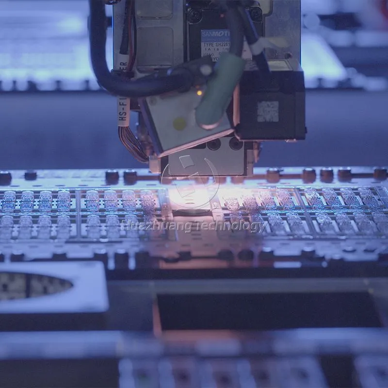
PCBA production yield is the percentage of assemblies that pass inspection and testing without requiring rework. A low first-pass yield increases:
For example, if a batch contains 10,000 PCB assemblies and the first-pass yield is 92%, approximately 800 boards may require rework or investigation. Even when most defective boards can be repaired, labor, testing, and component damage can significantly reduce margins.
In PCBA Contract Manufacturing, production yield is not controlled by one machine or one operator. It depends on the complete manufacturing system, including:
Huazhuang approaches yield improvement as a process-control project rather than a final inspection activity.
Before changing the process, I recommend creating a reliable baseline. Without accurate data, manufacturers may focus on visible defects while missing the actual source of yield loss.
Measure the following indicators for every production lot:
| KPI | Calculation | Recommended Use |
|---|---|---|
| First-Pass Yield | Passed units ÷ total tested units | Measures process stability |
| Rolled Throughput Yield | Product of yield at each process | Shows cumulative losses |
| Defects Per Million Opportunities | Defects ÷ opportunities × 1,000,000 | Compares product lines |
| Rework Rate | Reworked units ÷ total units | Measures hidden cost |
| Scrap Rate | Scrapped units ÷ total units | Identifies severe process failures |
| Defect Pareto | Defects ranked by frequency | Prioritizes corrective action |
Separate defects by process, such as solder bridging, insufficient solder, tombstoning, component shift, polarity error, open solder joints, and ICT failure.
Each PCB assembly should be linked to:
This traceability allows Huazhuang’s engineering team to identify whether a defect is related to a specific component lot, feeder, stencil aperture, machine head, or oven zone.
One of the most effective ways to improve PCBA Contract Manufacturing production yield is to identify design risks before the first board reaches the SMT line.
A DFM review should evaluate:
A 0.01 mm placement capability does not eliminate design-related defects. If the land pattern is incorrect or the pad spacing is too narrow, even a high-precision placement machine may produce bridging or skewed components.
During DFA review, check whether:
Huazhuang can use the Gerber files, ODB++ data, bill of materials, pick-and-place files, and assembly drawings to identify potential manufacturing risks before tooling and mass production.
Every ECO should be reviewed by engineering, quality, and production teams. Changes to component substitutes, PCB finishes, solder paste, stencil design, or reflow parameters can affect yield.
Use revision-controlled documents and obtain customer approval before implementing changes in production.
Material-related defects often appear to be process defects. In reality, damaged components, oxidized terminals, moisture-sensitive devices, and warped PCBs can create soldering failures that cannot be solved by machine adjustment alone.
Incoming PCB inspection should include:
For dimensional checks, use calibrated equipment with measurement resolution appropriate to the design, such as 0.01 mm for critical features where applicable.
For coatings and materials, applicable standards may include IPC-6012, IPC-A-600, and customer-specific specifications. Where coating adhesion is relevant, ASTM D3359 may be used as an additional test method. For quality management, ISO 9001 or DIN EN ISO 9001-based systems support documented control.
Component inspection should verify:
Moisture-sensitive devices should be stored and handled according to IPC/JEDEC J-STD-033. Components exposed beyond their allowable floor life may require controlled baking before assembly.
Solder paste should be controlled by:
Do not return used solder paste to unopened material. This can introduce contamination and alter rheological performance.
Solder paste printing is one of the most influential stages in PCBA yield improvement. Many downstream defects originate from incorrect paste volume or position.
Review:
For fine-pitch components, stencil aperture design should be calculated according to pad geometry and paste-release requirements. A poorly designed stencil may cause insufficient solder on thermal pads or solder bridging between fine-pitch leads.
Use solder paste inspection to measure:
A practical control plan may include SPI inspection at 100% of printed boards, especially for high-reliability or fine-pitch assemblies.
Corrective actions include:
The SMT line should be maintained with scheduled calibration and preventive maintenance. Check:
For advanced SMT equipment, placement precision may reach approximately 0.01 mm under controlled conditions, but actual performance depends on component size, board design, machine configuration, and maintenance status.
The reflow oven must deliver a thermal profile suitable for the solder alloy, PCB construction, and component package.
A profile should monitor:
Use thermocouples attached to representative locations, including:
The profile should follow the solder paste manufacturer’s technical data and relevant requirements from IPC-J-STD-020 and IPC J-STD-001.
| Defect | Likely Cause | Corrective Action |
|---|---|---|
| Tombstoning | Uneven heating or paste volume | Balance pads, adjust profile, inspect stencil |
| Solder bridging | Excess paste or misalignment | Reduce aperture, improve print alignment |
| Insufficient solder | Low paste volume or poor wetting | Review aperture and surface condition |
| Head-in-pillow | BGA warpage or oxidation | Control profile and component storage |
| Voiding | Thermal pad design or volatile release | Optimize aperture pattern and profile |
| Component shift | Uneven paste deposit or vibration | Check placement and board support |
Reflow profiling should be repeated after major changes to solder paste, PCB design, component package, oven maintenance, or conveyor settings.
Inspection should not wait until the final assembly stage. Huazhuang recommends a layered quality-control system.
A typical PCBA inspection route may include:
AOI is effective for detecting polarity errors, component presence, offset, solder bridges, and open joints. X-ray is particularly useful for BGA, QFN, LGA, and bottom-terminated components.
For high-risk assemblies, apply 100% AOI and functional testing. For lower-risk products, sampling may be used only after the process demonstrates stable capability and the customer approves the control plan.
Quality acceptance should be documented against the applicable class of:
These standards should be included in inspection instructions and operator training rather than referenced only during customer audits.
Inspection data improves yield only when the factory uses it to prevent recurrence.
When a defect exceeds the defined limit:
Huazhuang can establish a 24-hour response target for major production or quality issues, depending on the agreed service level and project requirements.
Do not attempt to correct every minor defect simultaneously. First address the small number of defect categories responsible for most yield loss.
For example, if solder bridging accounts for 38% of all defects and component polarity errors account for 22%, these two problems should receive priority over low-frequency cosmetic issues.
If operators record defects using inconsistent names, the Pareto chart becomes unreliable.
Solution: Create standardized defect codes, require photo evidence for major defects, and train inspectors to classify defects according to IPC-A-610 criteria.
Different PCB or component suppliers may use materials with different solderability, flatness, or dimensional tolerances.
Solution: Establish incoming inspection limits, supplier scorecards, approved vendor lists, and periodic supplier audits.
Frequent substitutions can disrupt validated SMT programs and reflow profiles.
Solution: Use formal ECN/ECO approval, conduct first-article verification, and update all machine libraries and inspection programs before release.
A repaired board may pass final inspection but still represent a process failure.
Solution: Report first-pass yield separately from final yield. Track rework hours, repair locations, and repeated defect types.
Incomplete BOM information, unclear acceptance criteria, and outdated drawings can create avoidable defects.
Solution: Confirm the latest BOM, Gerber files, assembly drawings, test specifications, revision level, and packaging requirements during the NPI process.
The right tools make process control faster and more objective.
Recommended resources include:
A manufacturing execution system can connect material lots, machine programs, inspection results, and operator records. This reduces manual reporting errors and shortens root-cause analysis.
Huazhuang combines engineering review, controlled production, inspection, and communication to help customers reduce avoidable PCBA defects. The goal is not simply to repair defective boards, but to prevent defects from being created.
A reliable PCBA Contract Manufacturing partner should provide:
When these controls are implemented consistently, PCBA Contract Manufacturing production yield becomes measurable, repeatable, and easier to improve.
To begin improving yield, I recommend that your team take these actions immediately:
By controlling the process from design release through final functional testing, manufacturers can reduce rework, shorten delivery cycles, and achieve more stable PCBA Contract Manufacturing production yield. With Huazhuang’s structured approach, How to Improve PCBA Production Yield becomes a practical manufacturing program rather than a one-time troubleshooting exercise.
A: To enhance PCBA production yield, begin by establishing a reliable baseline for yield metrics. Focus on DFM and DFA reviews, strengthen incoming material quality control, optimize SMT printing and placement, and implement a robust inspection and testing regime throughout the production process.
A: Huazhuang specializes in engineering review and controlled production processes that address common yield issues. We provide services including DFM support, BOM and component verification, and comprehensive inspection capabilities to minimize defects before they occur and ensure a measurable improvement in yield.
A: Key indicators include First-Pass Yield, Rolled Throughput Yield, Defects Per Million Opportunities, Rework Rate, and Scrap Rate. Monitoring these metrics allows for better analysis and targeted improvement efforts.
A: Certainly! We offer detailed specifications for all our components, ensuring they align with industry standards such as IPC-6012 and IPC-A-610, along with full traceability records to support your manufacturing needs.
A: Huazhuang implements a layered quality-control system that includes Solder Paste Inspection (SPI), Automated Optical Inspection (AOI), X-ray inspection, and Functional Testing to catch defects at multiple stages of the production process.
Guangdong Huazhuang Technology Co., Ltd.
+86 0769 8372 4262
No. 1, Taoyuan Road, Cunwei, Hengli Town, Dongguan City, Guangdong Province


